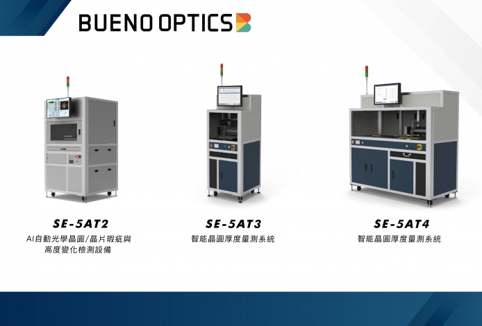
Intelligent Wafer Thickness Measurement System /Intelligent Optical Wafer Surface Defect and Height Variation Inspection Equipment

Intelligent Wafer Thickness Measurement System /Intelligent Optical Wafer Surface Defect and Height Variation Inspection Equipment

Manufacturer:BUENO OPTICS CO.,LTD

Special equipment for wafer defect, thickness and 3D information measurement and planning is still under research and development. In the product process parameter test, it is characterized by high availability, high measurement accuracy and stability.
DETAILS
The application of BUENO OPTICS optical technology has been extended to the semiconductor industry. It is integrated and developed with AI defect detection and 3D white light conjugate focus/interference module. Special equipment for wafer defect, thickness and 3D information measurement and planning is still under research and development. In the product process parameter test, it is characterized by high availability, high measurement accuracy and stability.
 
MORE SOLUTIONS
close Site-wide search
close
closeAppointment
Company booked for consultation:
Please ensure filling in accurate information.Required fields, incomplete forms will not be answered.
Business nameex : ○○ Co. Ltd.
Nameex : Jason
Departmentex : R&D Department
Job titleex : R&D Manager
Telex : 0212345678
Mobileex : 0911222333
E-mailex : Please enter E-mail
E-mail confirmationex : Please confirm E-mail
Objectex: Technical partnership, sales, procurement, OEM, overseas business expansion
Captcha
I have read and agree to the Privacy Policy PRIVACY POLICY
iconSubmit